
이미 소장하고 있다면 판매해 보세요.
- 국내배송만 가능
- 해외 거래처 사정에 의하여 품절/지연 가능
- 도서 정보 중 미표기 사항 안내?
- 문화비소득공제 가능
이 상품의 태그
-
상품명 이동Federated Learning with Python: Design and implement a federated learning system and develop applications using existing frameworks36,000원
-
상품명 이동Gas Turbine Design, Components and System Design Integration: Second Revised and Enhanced Edition10% 422,080원
-
상품명 이동Control System Design Guide: Using Your Computer to Understand and Diagnose Feedback Controllers10% 135,590원



책소개
목차
|
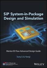
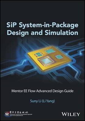
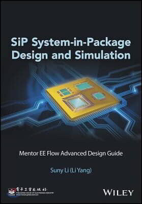
About the Author xiii Preface xv 1 SiP Design and Simulation Platform 1 1.1 From Package to SiP 1 1.2 The Development of Mentor SiP Design Technology 5 1.3 The Mentor SiP Design and Simulation Platform 6 1.4 The Introduction of the Finished Project 16 2 Introduction to Package 19 2.1 Definition and Function of Package 19 2.2 Development of Packaging Technology 20 2.3 SiP and Related Technologies 24 2.4 The Development of the Package Market 31 2.5 Package Manufacturers 32 2.6 Bare Chip Suppliers 35 3 The SiP Production Process 37 3.1 BGA: The Mainstream SiP Package Form 37 3.2 The SiP Package Production Process 39 3.3 Three Key Elements of SiP 41 4 New Package Technologies 45 4.1 TSV (Through Silicon Via) Technology 45 4.2 Integrated Passive Device (IPD) Technology 49 4.3 Package on Package (PoP) Technology 51 4.4 Apple A8 processor ? an Example of a PoP Product 55 5 SiP Design and Simulation Flow 59 5.1 SiP Design and Simulation Flow 59 5.2 Design and Simulation Process in Mentor EE Flow 61 6 Central Library 67 6.1 The Structure of the Central Library 67 6.2 Introduction to the Dashboard 68 6.3 Schematic Symbol Creation 70 6.4 Bare Chip Cell Creation 76 6.5 BGA Cell Creation 82 6.6 Part Creation 90 6.7 Create Cell Via Part 92 7 Schematic Input 97 7.1 Netlist Input 97 7.2 Basic Schematic Input 99 7.3 Schematic Input Based on DxDataBook 120 8 Multi-board Project Management and Concurrent Schematic Design 127 8.1 Multi-Board Project Management 127 8.2 Concurrent Schematic Design 130 9 Layout Creation and Setting 137 9.1 Create Layout Template 137 9.2 Create Layout Project 146 9.3 Layout-Related Setup and Operation 149 9.4 Substrate Layout 174 9.5 eDxD View 177 9.6 Input Chinese Characters in Layout 178 10 Constraint Rules Management 183 10.1 CES ? Constraint Editor System 183 10.2 Scheme 185 10.3 Define Layer Stackup and Parameters 187 10.4 Net Class 188 10.5 Clearance Rules 190 10.6 Constraint Class 194 10.7 Update CES Data with Layout 200 11 Wire Bond Design 201 11.1 Wire Bond Overview 201 11.2 Bond Wire Model 203 11.3 Wire Bond Toolbar 209 12 Cavity and Chip Stack Design 229 12.1 Cavity 229 12.2 Chip Stack 239 13 Flip Chip and RDL Design 249 13.1 The Concept and Characteristics of Flip Chip 249 13.2 The RDL Concept 250 13.3 RDL Design 250 13.4 Flip Chip Design 260 14 Route and Plane 269 14.1 Routing 269 14.2 Plane 291 15 Embedded Passives Design 303 15.1 The Development of Embedded Technology 303 15.2 Process and Material for Embedded Passives 305 15.3 Resistor and Capacitor Automatic Synthesis 319 16 RF Circuit Design 331 16.1 RF SiP Technology 331 16.2 Mentor RF Design Flow 332 16.3 RF Schematic Design 333 16.4 RF Parameter Transfer Between Schematic and Layout 342 16.5 RF Layout Design 344 16.6 Connect RF Simulation Tools and Transfer Data 363 17 Concurrent Layout Design 367 17.1 Concurrent Layout Design Technology ? Xtreme 367 17.2 Xtreme Configuration 369 17.3 Start Xtreme Concurrent Design 371 17.4 Matters to Note in Xtreme 375 18 3D Real-time DRC 377 18.1 Wire Model Editor 3D Display and DRC 377 18.2 3D Viewer Display and DRC 380 19 Design Review 395 19.1 Online DRC 395 19.2 Batch DRC 395 19.3 Review Hazards 401 19.4 Verify Design Library 403 20 Manufacturing Data Output 407 20.1 Drill and Gerber Data Output 407 20.2 Other Manufacturing Data Output 416 21 SiP Simulation Technology 425 21.1 SiP Simulation Technology Overview 425 21.2 Signal Integrity Simulation 426 21.3 Power Integrity Simulation 436 21.4 Thermal Analysis 443 21.5 EMI/EMC Analysis 457 21.6 Mixed-Signal Simulation Introduction 462 Reference Materials 467 Postscript and Thanks 469 Index 471 |
저자 소개
Mr. Suny Li (Li Yang) is a SiP/PCB Technical Specialist in China; he now works in AcconSys Technology Co. Ltd, (a Mentor Authorized Distributor for China). Suny has guided and consulted on dozens of SiP projects in China, accumulating plentiful experience in SiP design and simulation. Suny has 10 years' experience in and knowledge of Application Engineer for Mentor, especially in SiP/PCB design and simulation. Before this, Suny worked in the Chinese Academy of Science and SIEMENS for several years. He has more than seven years' experience in hardware design (HW system design, PCB layout, high?speed signal integrity, power integrity, EMI, etc.). In the course of his work, Suny has published papers and acquired four patents, and he continues with this work. Suny is a senior member of the Chinese Institute of Electronics (CIE) and a member of the IEEE. Suny graduated from Beijing University of Aeronautics & Astronautics (BUAA) in 2000, receiving Master's and Bachelor's degrees in Science and Technology of Aeronautics & Astronautics.
품목정보
- 발행일
- 2017년 07월 24일
- 쪽수, 무게, 크기
- 400쪽 | 168*249*30mm
- ISBN13
- 9781119045939
사락 별점0
혜택 및 유의사항밑줄0
혜택 및 유의사항상품정보안내
(판형과 판수 등이 다양한 도서는 찾으시는 도서의 ISBN을 알려 주시면 보다 빠르고 정확한 안내가 가능합니다.)
해외거래처에서 품절인 경우, 2차 거래선을 통해 유럽과 미국 출판사로 직접 수입이 진행될 수 있습니다.
수입 진행 시점으로 부터 2~3주가 추가로 소요되며, 해외에서도 유통이 원활하지 않은 도서는 품절 안내가 지연될 수 있습니다.
해당 경우, 문자와 메일로 별도 안내를 드리고 있사오니 마이페이지에서 휴대전화번호와 메일주소를 다시 한번 확인해주시기 바랍니다.